Advanced PCB Design Techniques for High-Speed Digital Circuits
Master the art of high-speed PCB design with comprehensive coverage of signal integrity, power distribution, EMI reduction, and advanced routing techniques for modern digital systems.

Advanced PCB Design Techniques for High-Speed Digital Circuits
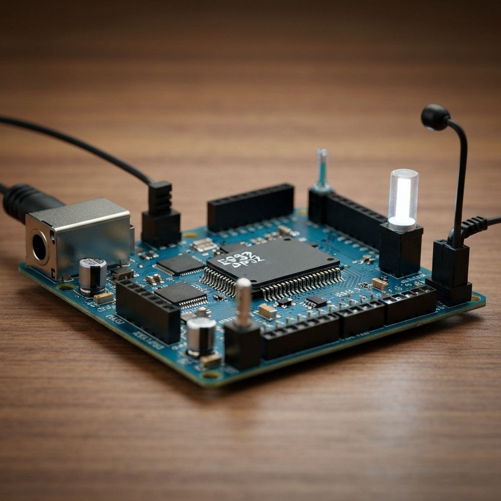
In today's world of high-performance electronics, proper PCB design is crucial for signal integrity and system reliability. This comprehensive guide covers advanced techniques for designing PCBs that handle high-speed digital signals with minimal interference and maximum performance.
Understanding High-Speed Digital Design Challenges
High-speed digital circuits present unique challenges that don't exist in traditional low-frequency designs:
Signal Integrity Issues
- Reflection: Impedance mismatches cause signal reflections
- Crosstalk: Adjacent traces interfere with each other
- Ground Bounce: Simultaneous switching causes voltage fluctuations
- Jitter: Timing variations in clock signals
Transmission Line Theory in PCB Design
Characteristic Impedance
For a microstrip trace on a PCB:
Z₀ = 87/√(εᵣ + 1.41) × ln(5.98h/(0.8w + t))
Where:
- Z₀ = Characteristic impedance (Ω)
- εᵣ = Dielectric constant
- h = Dielectric height
- w = Trace width
- t = Trace thickness
Layer Stack-up Design
4-Layer Stack-up Example
Layer 1: Signal (Top)
Layer 2: Ground Plane
Layer 3: Power Plane
Layer 4: Signal (Bottom)
Dielectric Selection: Use low-loss materials like Rogers RO4350B for frequencies above 1 GHz.
Advanced Routing Techniques
Length Matching
Critical for maintaining timing relationships in high-speed digital systems. DDR memory interfaces require trace length matching within ±25 mils for optimal performance.
Via Management
Minimize via usage in high-speed paths. Via inductance can be calculated as:
L_via = 5.08 × h × [ln(4h/d) + 1]
Where h is via barrel length and d is drill diameter.
Power Distribution Network (PDN) Design
Decoupling Strategy
Multi-decade decoupling approach:
- Bulk Capacitors: 100-1000µF (low frequency)
- Ceramic Capacitors: 0.1-10µF (mid frequency)
- High-Frequency Capacitors: 1-100nF (high frequency)
EMI/EMC Considerations
Electromagnetic Compatibility Rules
- Current Return Paths: Always provide low-impedance return paths
- Loop Area Minimization: Reduce the area enclosed by current loops
- Proper Termination: Match impedances to minimize reflections
Case Study: DDR4 Memory Interface
Signal Groups and Requirements
DDR4 Signal Groups:
- Clock (CK/CK#): Differential, length-matched
- Address/Command: Single-ended, length-matched within group
- Data (DQ): Length-matched within byte groups
- Data Strobe (DQS/DQS#): Differential, length-matched to DQ
Routing Strategy
- Layer Assignment: Use adjacent signal layers with dedicated power/ground
- Length Matching: ±25 mils for clock, ±250 mils for data groups
- Via Minimization: Direct routing preferred, maximum 2 vias per net
Best Practices Summary
- Start with Stack-up: Define controlled impedance early
- Simulate Early: Use field solvers for critical nets
- Minimize Discontinuities: Avoid unnecessary vias and stubs
- Plan Return Paths: Ensure continuous reference planes
- Validate Design: Use measurement tools to verify performance
Conclusion
High-speed PCB design requires careful consideration of electrical, mechanical, and manufacturing constraints. Success depends on understanding the physics of signal propagation, implementing proper design rules, and validating performance through simulation and measurement.
Key Takeaway: Good high-speed PCB design is about controlling the electromagnetic environment in which your signals propagate. Master these fundamentals, and your designs will perform reliably at gigahertz frequencies.
Tags

Manish Bookreader
Electronics enthusiast, Embedded Systems Expert, Linux/Networking programmer, and Software Engineer passionate about AI, electronics, books, and cooking.